Fast AFM array technology for
semiconductor metrology
Atomic force microscopy (AFM) is the gold standard for Z-axis measurement, but it is too slow for high-volume manufacturing.
icspi’s AFM array technology enables extreme throughput and unprecedented wafer coverage with AFM.
TECHNOLOGY
Our AFM array technology uses miniaturized 1 mm2 AFM scan heads in parallel. Each scan head is an entire MEMS-based AFM.
- Extremely scalable: entire AFM functionality packed onto a 1 mm2 scan head
- Navigate to targets: each scan head has 3-axis control for fine positioning and scanning
- Low overhead: eliminate laser alignment with on-chip sensing
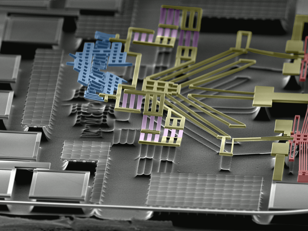
AFM scan head with 3-axis movement and on-chip sensing.
BENEFITS
AFM array technology enables chipmakers to achieve:
- Faster time-to-yield and faster time-to-market
- One-shot full wafer AFM metrology
- Die-to-die hotspot comparison
- Potential for inspection with AFM
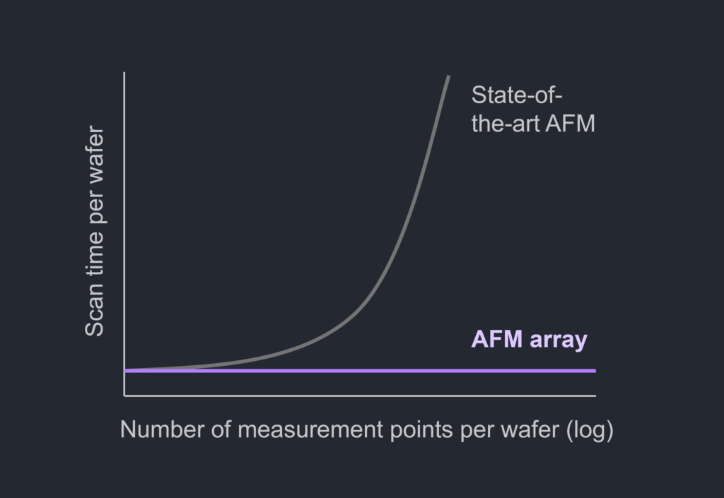
Scale the number of measurement points per wafer without increasing scan time using AFM arrays.
Contact Us
Interested to learn more about how AFM array technology can accelerate your time-to-yield?
Follow the link below to request more information about AFM array technology.