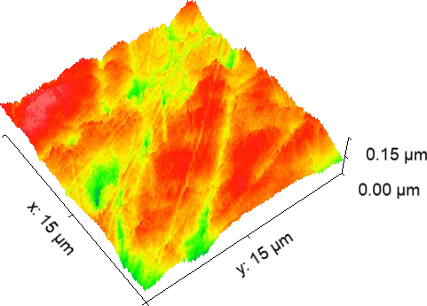
Can AFM measure surface roughness?
Measuring surface roughness with atomic force microscopy (AFM)
When it comes to investigating the roughness of various materials, there is one technique that stands out above the rest — atomic force microscopy (AFM). In this blog post, we will delve into the realm of AFM and explore how it offers unparalleled capabilities in examining the surface characteristics of different objects.
AFM works a bit like a record player: using a sharp probe to scan across the surface of a sample. It does this at extremely high resolution and detects even the smallest variations in surface topography.
AFM measures interaction forces between the tip and sample, and converts this into topography data. The interaction forces are extremely tiny, so AFM collects data down to the nanoscale or even lower! AFM is ve Because it is a physical technique, virtually any solid sample can be scanned. So whether you’re investigating a silicon wafer or examining the rugged terrain of a bacterium, AFM has got you covered.

AFM doesn’t just tell you if a surface is smooth or rough; it quantifies the roughness down to the nanoscale level. Researchers, engineers, and scientists rely on AFM to characterize surfaces for applications ranging from microelectronics to biotechnology. The reason is that AFM provides high-fidelity, high-resolution 3D data on virtually any solid surface.
How do you quantify surface roughness?
Surface roughness is a component of the texture of a surface: a higher value means that the surface is rougher. The arithmetic roughness (Ra) and the root-mean-squared roughness (Rq) are common parameters used to describe roughness.
Some examples of approximate surface roughnesses:
Silicon wafer: <1 nm rms
Optical material: <20 nm rms
Mirror finish: 100 – 200 nm rms
Satin finish: 1 – 2 μm rms
Rough, equivalent to polish with 60 grit: 6 μm rms
AFM compared to other techniques for roughness
Certain techniques, such as stylus profilometry, collect 2D topography data by moving across a line. Because AFM collects data in all three dimensions, the surface roughness can be calculated from the entire 3D scan area. The 2-d/area roughness parameters are arithmetic (Sa) and RMS (Sq).
In addition, AFM probes are much sharper than profilometer styli, so the lateral resolution is much higher than other contact techniques. Similarly, some optical profilers can collect 3D data, but the lateral resolution is limited by the wavelength of light.
Techniques like optical microscopy or scanning electron microscopy (SEM) cannot collect roughness directly, but there are ways to approximate the surface roughness using these techniques.
Breaking Taps Video on the Smoothest Materials
A popular video from the YouTube channel Breaking Taps sheds light on the roughness of six different items possessing varying degrees of smoothness. The journey starts with a gauge block, which, despite being precision ground, exhibits noticeable grinding marks and an average roughness of 11 nm rms. Other materials like a lambda/20 mirror blank, silicon wafer and glass slide are also scanned. All the samples are scanned with an nGauge atomic force microscope.

Interested in learning more about AFM?
Speak with an application engineer today to see how AFM can help with your research and process development.
