AFM for Thickness Measurement

Measuring thin film thickness is critically important in many scientific and industrial applications, as it provides essential insights into product performance and potential enhancements in manufacturing processes, leading to improvements in quality and cost-effectiveness. Atomic Force Microscopy (AFM) stands out as an exceptionally versatile tool for measuring and analyzing thin film thicknesses. Its high resolution, minimal requirements for sample preparation, and non-destructive nature make it particularly valuable.
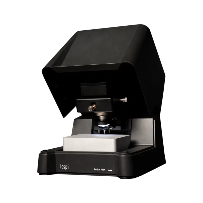
The nGauge and Redux Atomic Force Microscopes are notable in this domain, combining unparalleled precision, flexibility, and user-friendliness for thin film analysis. Their ability to accurately measure film thicknesses ranging from single-digit nanometers to 10s of micrometers make them indispensable for both research and industry.
AFMs offer a significant advantage over traditional contact profilometers, which are confined to single-dimensional data collection. In contrast, AFMs excel at providing detailed three-dimensional topographical information. This is particularly beneficial when examining thin films, as it allows for a comprehensive understanding of the film’s uniformity, surface characteristics, and potential flaws. Such thorough data is crucial in a range of applications, from semiconductor manufacturing to materials science research.
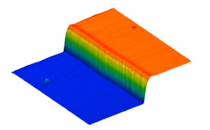
The proficiency of our AFMs in thin film measurement is demonstrated in their application for analyzing a silicon device with an anticipated top layer thickness of 520 nm. Although the lateral range of these instruments is generally smaller than that of a profilometer, this does not take away from their usefulness as a tradeoff is better resolution. The integrated optical microscope and XY stage on the Redux model facilitate easy and accurate alignment of the AFM’s tip with specific regions of interest, an essential step for reliable thin film measurement.
During the examination of the silicon device, the AFM exhibited its remarkable capabilities. Not only did it confirm the expected film thickness, but it also detected minuscule surface contaminants. Unlike profilometry, where a single contaminated line profile might compromise the accuracy of the measurement, the AFM’s ability to scan multiple areas and select a clean section for analysis ensures the validity of the measurements. This feature greatly reduces the need for repetitive measurements, thus improving efficiency and productivity.
Additionally, the AFM provides in-depth data on the surface characteristics of thin films, such as texture and uniformity, as well as detailed information on sidewall features like slope and profile. These insights are invaluable for optimizing manufacturing processes and ensuring the quality of thin films. In situations where precise control of film thickness is essential, the detailed three-dimensional data offered by AFM represents a significant advantage over conventional measurement methods like profilometry.
| Desktop AFM | Stylus (contact) profilometer | White light interferometer (3D optical profiler) | |
|---|---|---|---|
| Time to Data | Fast | Fast | Fast |
| Sample Requirements | Any solid sample | Any solid sample | Opaque and optically reactive |
| 3D Data? | ✔ | ✖ | ✖ |
| Direct Measurement? | ✔ | ✔ | ✖ |
In summary, AFMs are formidable instruments for the measurement of thin film thickness. Their advanced capabilities in delivering detailed three-dimensional topographical data, combined with precision and ease of use in our products, make them essential tools for both scientific research and industrial applications.
Our AFMs – the nGauge and Redux – surpass traditional profilometry in providing richer, more accurate data, and enhance the efficiency and reliability of thin film measurements, solidifying their role as critical technologies in the field of nanoscale material analysis.
Compared to legacy AFMs, our systems provide much faster time-to-data combined with greater ease of use in a small form-factor. Our systems do away with traditional laser alignment and manual approach systems in favour of an automated micro-electromechanical-based system (MEMS) that greatly reduces the burden on the user. Our AFMs can live right on your benchtop and help you unlock your full capabilities.
Speak with an expert
Interested to learn more about how AFM can provide insight on the thickness of your thin film samples at the nanoscale?

